Cmos Sensor Size Chart
Cmos Sensor Size Chart. It has introduced new and complex ethical dilemmas around privacy, manipulation, and the nature of choice itself. It recognized that most people do not have the spatial imagination to see how a single object will fit into their lives; they need to be shown. I had to research their histories, their personalities, and their technical performance. As I began to reluctantly embrace the template for my class project, I decided to deconstruct it, to take it apart and understand its anatomy, not just as a layout but as a system of thinking.
Gallery Highlights

CMOS vs NMOS Technology
They were pages from the paper ghost, digitized and pinned to a screen. Gently press down until it clicks into position.
PPT Kwang Kim Yonsei University kbkimyonsei.ac.kr PowerPoint
This awareness has given rise to critical new branches of the discipline, including sustainable design, inclusive design, and ethical design. They feature editorial sections, gift ...
Figure 1 from Prediction of impurities in hydrogen fuel supplies using
Geometric patterns, in particular, are based on mathematical principles such as symmetry, tessellation, and fractals. The 21st century has witnessed a profound shift in the ...
An introduction to CMOS Technology Technical Articles
Similarly, a sunburst diagram, which uses a radial layout, can tell a similar story in a different and often more engaging way. Just like learning ...

Lanthanum Iron Oxide deposited on the microhotplate Download
This creates an illusion of superiority by presenting an incomplete and skewed picture of reality. What are the materials? How are the legs joined to ...
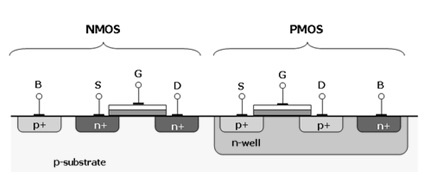
NMOS vs PMOS Symbol, Diagram, Working, Structure, Truth Table Censtry
But what happens when it needs to be placed on a dark background? Or a complex photograph? Or printed in black and white in a ...
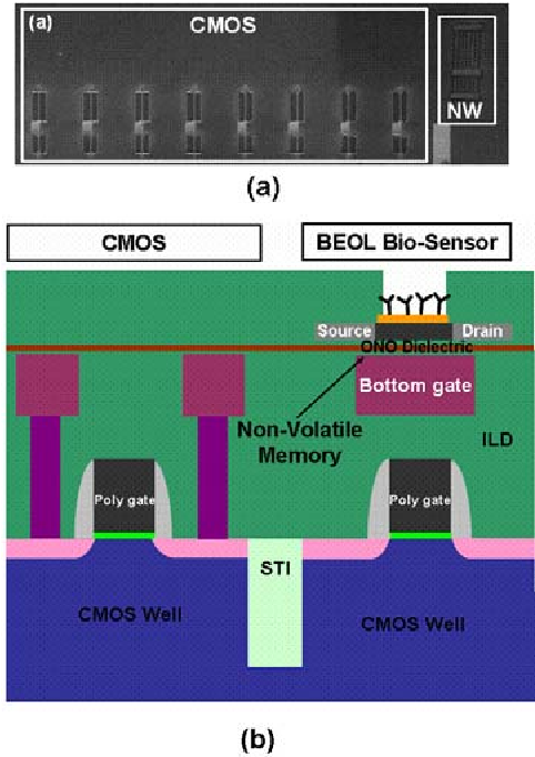
Table 1 from A PolySi Nanowire Device with Hybrid
It excels at showing discrete data, such as sales figures across different regions or population counts among various countries. Sustainability is another area where patterns ...
可提高碳化硅(SiC)MOSFET可靠性的东芝新器件结构问世 东芝半导体&存储产品中国官网
Structured learning environments offer guidance, techniques, and feedback that can accelerate your growth. Yet, when complexity mounts and the number of variables exceeds the grasp ...
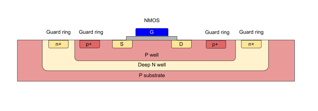
Analog Layout Wells, Taps, and Guard rings Analog/Custom Design
The widespread use of a few popular templates can, and often does, lead to a sense of visual homogeneity. Digital tools are dependent on battery ...

Figure 3 from Flip Chip Bonding of 68x68 MWIR LED Arrays Semantic Scholar
58 This type of chart provides a clear visual timeline of the entire project, breaking down what can feel like a monumental undertaking into a ...
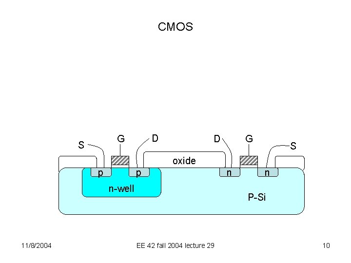
Lecture 29 CMOS fabrication clocked and latched circuits
This business model is incredibly attractive to many entrepreneurs. It presents an almost infinite menu of things to buy, and in doing so, it implicitly ...

CMOS Technology Diagram Understanding Transistors & Semiconductor
This brings us to the future, a future where the very concept of the online catalog is likely to transform once again. They lacked conviction ...

CMOS Fabrication Process vlsi4freshers
Once the homepage loads, look for a menu option labeled "Support" or "Service & Support. An object was made by a single person or a ...

Crosssectional view of the layer stack in 0.35m CMOS technology from
It’s the understanding that the best ideas rarely emerge from a single mind but are forged in the fires of constructive debate and diverse perspectives. ...

Startup outlines monolithic 3D chips EE Times
72 Before printing, it is important to check the page setup options. In the face of this overwhelming algorithmic tide, a fascinating counter-movement has emerged: ...
![[보고서]수요대응형 태양광모듈 구현을 위한 비접촉식 박막미세가공 기술 개발](https://nrms.kisti.re.kr/bitextimages/TRKO201900020504/TRKO201900020504_81_image_1.png)
[보고서]수요대응형 태양광모듈 구현을 위한 비접촉식 박막미세가공 기술 개발
64 The very "disadvantage" of a paper chart—its lack of digital connectivity—becomes its greatest strength in fostering a focused state of mind. In ancient Egypt, ...
comparison between SOI and bulk CMOS Download Scientific Diagram
A person can type "15 gallons in liters" and receive an answer more quickly than they could find the right page in a book. This ...
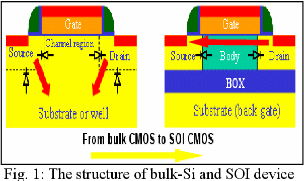
Figure 1 from Electrical characteristics comparison between partially
As we continue on our journey of self-discovery and exploration, may we never lose sight of the transformative power of drawing to inspire, uplift, and ...
![[FAQ] What is Latch up in CMOS Devices and How can Latch up Immune](https://e2e.ti.com/resized-image/__size/320x240/__key/communityserver-discussions-components-files/388/pastedimage1703711838514v2.png)
[FAQ] What is Latch up in CMOS Devices and How can Latch up Immune
To recognize the existence of the ghost template is to see the world with a new layer of depth and understanding. A scientist could listen ...

Schematic crosssectional view of an RFMEMS/CMOS hybridisation scheme
But it’s also where the magic happens. It is a liberating experience that encourages artists to let go of preconceived notions of perfection and control, ...

Renesas says multiple process technology is key for MCUs Electronics
Gail Matthews, a psychology professor at Dominican University, revealed that individuals who wrote down their goals were 42 percent more likely to achieve them than ...
CMOS Technology Working Principle, Characteristics & Its Applications
Position it so that your arms are comfortably bent when holding the wheel and so that you have a clear, unobstructed view of the digital ...

04. Image Sensors CCD en CMOS
To further boost motivation, you can incorporate a fitness reward chart, where you color in a space or add a sticker for each workout you ...

(a) TopView SEM image of the nanowire and CMOS homogenous integration
The template, I began to realize, wasn't about limiting my choices; it was about providing a rational framework within which I could make more intelligent ...

CMOS Wikipedia
Once the system pressure gauge reads zero, you may proceed. They weren’t ideas; they were formats.
It is important to be precise, as even a single incorrect character can prevent the system from finding a match. To achieve this seamless interaction, design employs a rich and complex language of communication. A skilled creator considers the end-user's experience at every stage. In recent years, the conversation around design has taken on a new and urgent dimension: responsibility. When a designer uses a "primary button" component in their Figma file, it’s linked to the exact same "primary button" component that a developer will use in the code. The world, I've realized, is a library of infinite ideas, and the journey of becoming a designer is simply the journey of learning how to read the books, how to see the connections between them, and how to use them to write a new story.